Having available the two techniques, when to coat with gold and when with carbon?
Even though the graphite thread preparation is something more laborious, both processes are carried out in a very simple way and the images obtained with both techniques are comparable, being more critical the effect produced on the microanalysis. In the spectrums obtained from the coated specimens, it will be obvious the presence of peaks of gold or carbon that have been previously deposited. This inconvenient is solved by a simple indication that the sample has been covered for the corresponding analysis.
Whatever might be the selected technique, diverse non-conductive materials can be as well perfectly analyzed in the IK4-AZTERLAN Scanning Electron Microscopes by coating the samples as explained before.
Accurate images and qualitative analyses of the samples are obtained as a result of these specific characterizations. In the case of non-metallic materials whose transformation processes might be away from our main level of expertise, the combined work with the technicians from our customer companies is remarkable, adding the capabilities of our respective specialties; bringing together the knowledge of the manufacturing processes, the properties of the materials, along with the capabilities of the Scanning Electron Microscopy techniques and precise analytical methods.
-
- Follow Us
- —
IK4-AZTERLAN is a technology Center specialized in metallurgy. The internal level of expertise and most of the materials involved in the daily work have therefore a metallic nature. Nevertheless and due to the versatility offered by the Scanning Electron Microscopy techniques there are very different types of materials that can be analyzed in this kind of equipments. Among them, we can mention materials such as glass, plastics, rubber, wood conglomerates, paintings, sands, refractory materials, … etc.
The analysis of this type of materials is possible since the equipment has three different modes of vacuum: high vacuum, for conductive samples; controlled pressure, for samples that do not conduct electricity and the environmental pressure, for biological samples.
Whatever nature might have the material to be analyzed, it must be always solid and clean, and completely free from dust. In the case that the samples are not in solid state (paintings, for example), there is always the possibility of drying a portion of the product on the stove and analyze its dry residue.
Unlike in the optical microscopes where the light is formed by a conventional lamp, the light source of the scanning electron microscopes consists on a beam of electrons which are electromagnetically accelerated and impact on the sample to be analyzed. The magnifications obtained by the equipment are inversely proportional to the wavelength of the lighting used; wavelength of the electrons is much lower than the visible light used in optical microscopes. Therefore, the use of this source of lighting makes possible to achieve major resolutions, which combined with their greater depth of field allow to obtain very detailed images with volume effect.
A characteristic of the metallic materials we usually work with is that they have a good electrical conductivity, which is one of the necessary characteristics to be able to be analyzed by the scanning electron microscopy technique.
If the sample to be analyzed is conductive, the received beam of electrons dissipate through the own sample allowing a correct scanning of its surface and making possible to obtain a good final image.
In the case of non-conductive samples, such as the non-metallic materials mentioned above, the electrons not will be evacuated through them, so the irradiated surface remains negatively charged. When continuing with the scanning of the sample, the electrons present on the surface will repel the new electrons that reach the sample (with a more negative charge) so the undesired “charging effect” will not allow the formation of a correct image in the microscope.
This problem can be solved in two different ways. Acting on the sample to make it electrically conductive or generating a conductive atmosphere around the sample which will dissipate the negative charge that receives from the beam. The last possible solution can be achieved using the second vacuum mode provided by the controlled pressure of the equipment. Water vapor is injected, creating a conductive medium through which the electrons of the bombarded surface are evacuated avoiding the “charging effect”.
This way of controlled pressure has been widely used in IK4-AZTERLAN for the analysis of non-conductive samples obtaining acceptable results. Anyhow, the previous experiences have shown us that except in absolutely indispensable cases, it is better to avoid this procedure mainly for two reasons:
- The high pressure on the column used in conductive samples is the best for proper targeting of electrons over the sample. In this particular case, the pressure used is much lower (around 0,5 bar) so electrons are dispersed more easily. This fact has a direct effect on the obtained spectrum which is not so accurate and might not correspond exactly with what we want to analyze.
- After the analysis of samples using this mode of vacuum, there is an accelerated degradation of the column, which has a direct impact on the quality of the image.
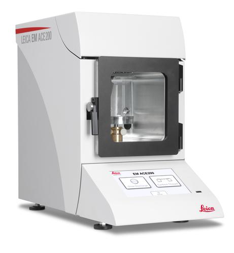
Due to these facts IK4-AZTERLAN has chosen to solve the problem making the samples electrically conductive by means of a sputter deposition process. This kind of device allows coating the surface of the samples with a fine enough layer (few nanometers) of an ultra-thin coating of electrically-conducting material that will be able to evacuate the electrons accumulated on the surface of the specimen during the electron irradiation required for imaging.These coatings are deposited using two different techniques: the evaporation of carbon and the metallic sputtering with noble metals. IK4-AZTERLAN has recently acquired a LEICA EM ACE200 equipment, able to work with both techniques.

The carbon evaporator consists of a thread of graphite that will facilitate the deposition of carbon layers on the sample up to 40 nm thick by a pulse evaporation procedure. Historically, this technique has been quite problematic as the carbonized graphite thread used to break easily, depositing itself on the sample and polluting its surface.
This problem is perfectly solved in this equipment, since electrical charges occur in the form of pulses, avoiding the graphite thread to break.
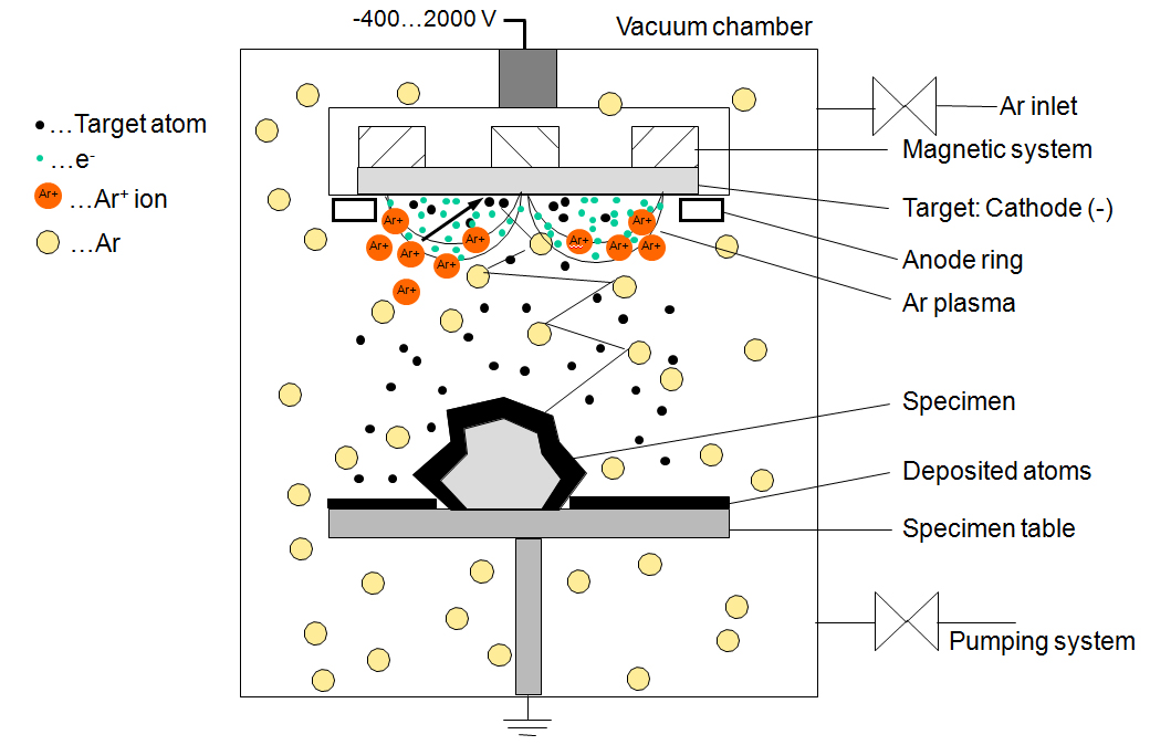
The metallic sputtering is done with gold in our particular case. As shown in the following figure the gold particles are deposited on the surface of the sample by passing an electric current through the gold target and within an argon atmosphere with a certain degree of depression.


